
Semiconductor
SEOUL Engineering will shape the future with endless challenges and innovations.
-
-
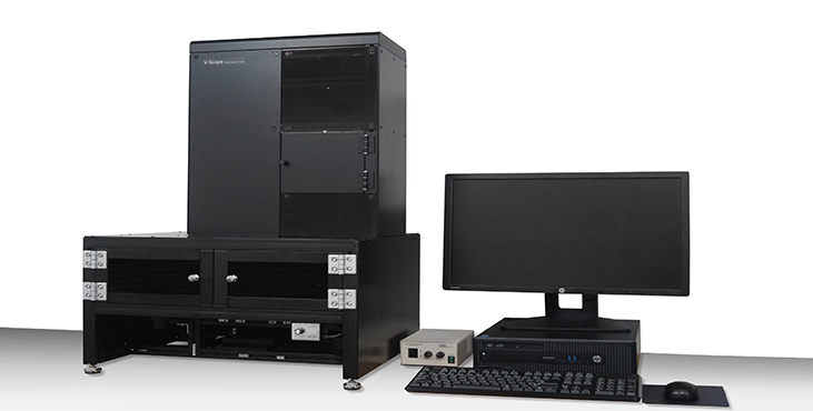
제품소개 product name NSV 50/100/200 Detail • NSV series with FOV(Field Of View)
- NSV 50 : FOV = 50 x 50mm
- NSV 100 : FOV = 100 x 100mm
- NSV 200 : FOV = 200 x 200mm
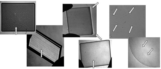
• Surface defect : Orange feel and wheel mark of Bare boards(Glass, Crystal and Sapphire etc.)
• Inspection before the vapor deposition of bare board
• Internal defect(stria, growth strip) at the tie of before shipment and acceptance inspection
• Irregularyobservation of the having many kinds of film
• The surface defect observation of the wafer: crack, dimple and wheel mark etc
• Various flatform possible depends on apllication : system for semiconductor and FPD equpment
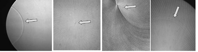
Saw marks (Polishing marks) : This saw mark can cause the crack on sample
Stria (inside defect) and Orange peel (surface defect) of Glass, Quartz, Crystal etc.
V-scopecan observe inside defect of transparent samples and surface defect of polishing marks.
These are impossible to observe by naked eyes.
